Streamlining Data Flow: Core Software Functionality Completed!

We have previously announced the PCB design is completed and boards are sent to manufacturing. Fabricated PCB boards have arrived! However, while we're all set to begin assembly, some key components are still coming. While we await the arrival of some essential elements, we've shifted our focus to completing the data streaming functionalities. Completing this core software functionality is a major milestone, bringing us closer to achieving all the project's core functionalities. Once the remaining components are received, we can proceed with the final assembly and testing.
This post dives into the details of how the voltage and current streaming feature works. We'll begin by focusing on the firmware implementation, followed by a detailed look at the GUI application development. We'll also point you to the relevant code in our GitHub repository for easy reference. To conclude, we'll showcase a short video presentation demonstrating the developed streaming functionalities.
Figure 1 illustrates all firmware software blocks that are parts of streaming functionalities.
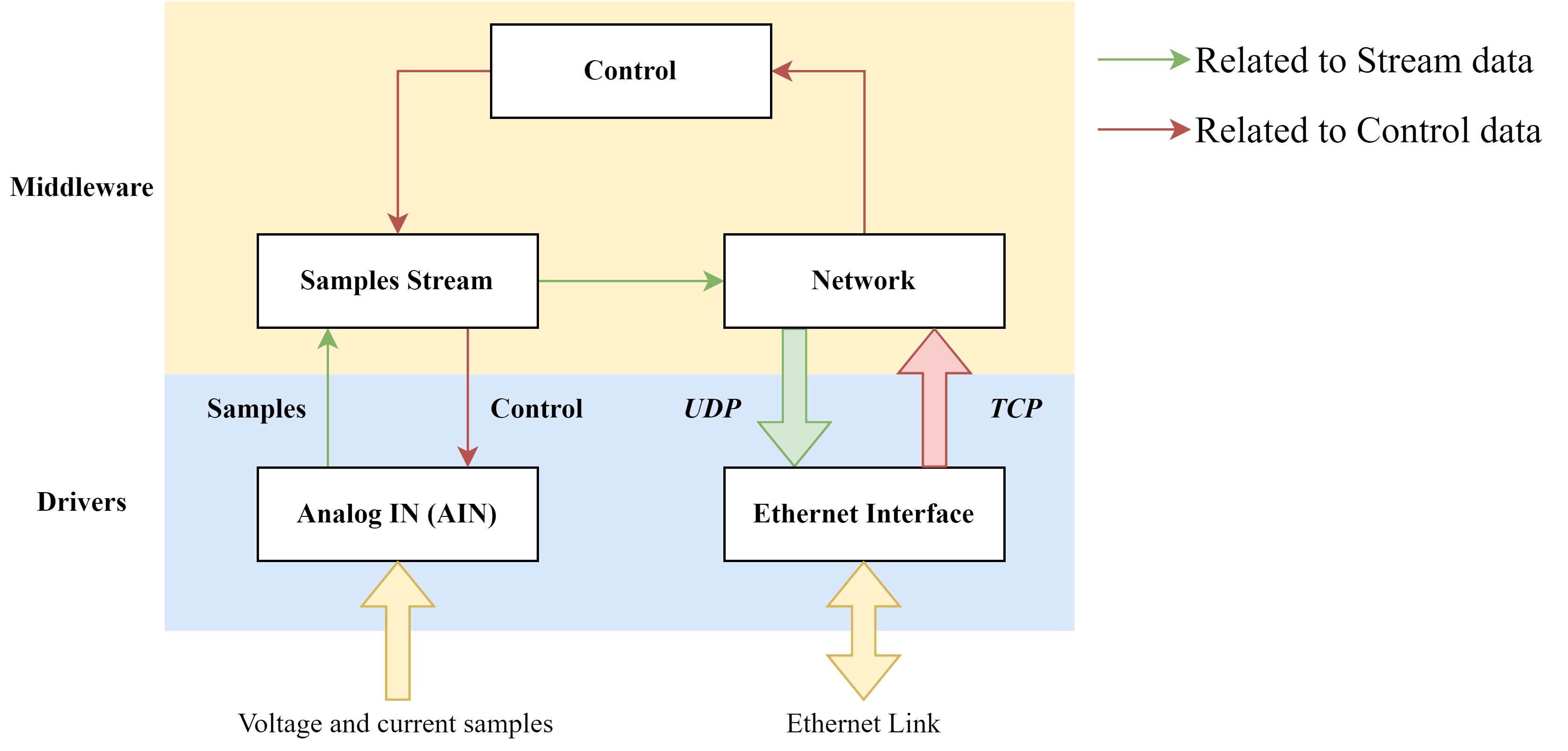
Presented blocks are:
Presented blocks are:
Firmware side of data streaming logic – main working principles
After MCU firmware is successfully run and the ethernet link is established, the host initiates the data streaming process by transmitting a control message. This message, as defined within the Commands Description file, contains the server’s IP address where obtained samples should be sent. This established streaming channel facilitates the continuous transmission of data from the MCU to the server for real-time processing or further analysis. For clarity, the "create stream" command format with some IP address information is provided below:
device stream create -ip=192.168.1.200 -port=5000
Upon receiving the control message, the Control Service parses it and forwards the "Create Stream" action to the Samples Stream Service . This service, based on the message content, creates a stream for sending data to the server at 192.168.1.200, port 5000.
The main service task, implemented within the prvSSTREAM_ControlTaskFunc function, handles the "Create Stream" command. Each established stream triggers the creation of a separate FreeRTOS task. This task efficiently gathers samples from underlying software layers, performs any necessary processing, and transmits the data to the previously defined server IP. When a stream is created, a Unique stream ID (SID) value is assigned to each stream, and it is used by stream-related commands to reference specific streams. This architecture facilitates the establishment of multiple concurrent streams, enabling the system to handle diverse data types and target various servers simultaneously. However, for testing purposes, this software version creates a single stream specifically for acquiring and transmitting voltage and current samples.
Following stream creation, the host can send commands for configuring parameters like sampling rate and resolution. The current software version supports the configuration of the following stream parameters:
The Commands Description file provides a comprehensive list of commands used to configure specific parameter values.
After the data stream is established and configured, the host may trigger data transmission by sending a "Start Stream" command. Upon receiving this command, the Stream Service leverages the Stream ID (SID) value to identify the relevant stream. The designated stream then begins continuous sample acquisition and transmits the data to the pre-configured server. This ongoing data transmission process can be dynamically controlled by the host through specific pause or stop commands.
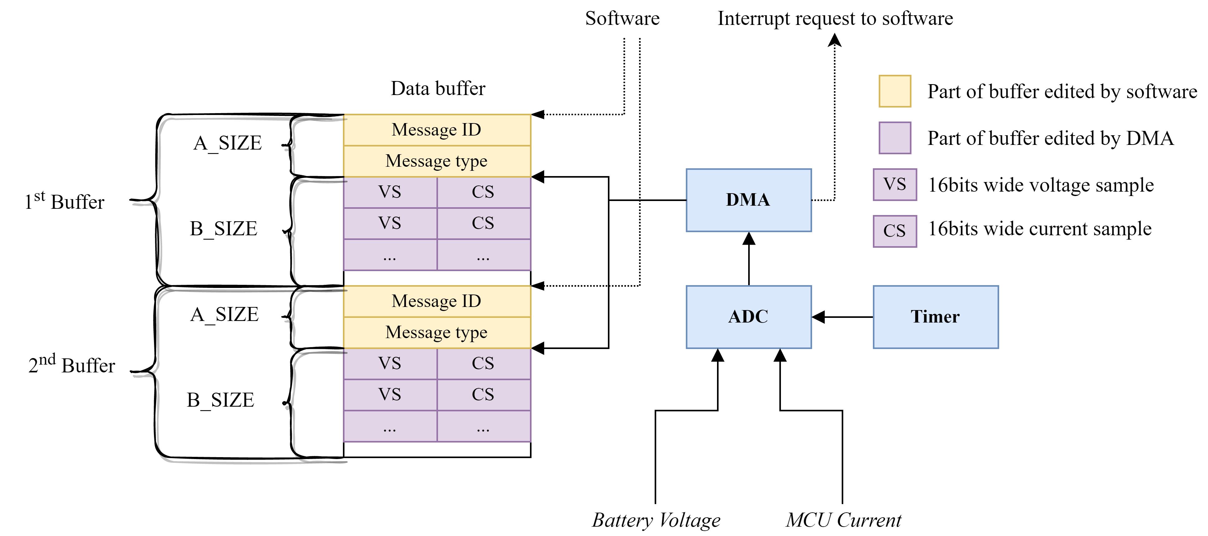
Continuous voltage and current sample acquisition is implemented within the Analog IN driver’s software block whose main components are illustrated in Figure 2. This software block utilizes different peripherals to continuously, with minimal software assistance, acquire and store multiple voltage and current samples into a single packet of data. For such actions, the Timer and DMA peripherals – both connected with ADC. Timer peripheral is configured to periodically, with a period defined by the host side with corresponding control command, trigger sample conversion. Voltage and current sampling are performed sequentially after the request to start conversion. Each end of the sampling process triggers DMA to store voltage current samples to the specific part inside MCU memory. An interrupt is generated when the buffer is filled with several samples defined with the DRV_AIN_ADC_BUFFER_MAX_SIZE macro. Inside ISR is called the previously registered callback function from the Samples Stream service which is forwarded buffer address value.
The corresponding stream task is triggered for further processing when current and voltage samples are stored inside a corresponding buffer. This processing logic implemented inside this task includes two steps:
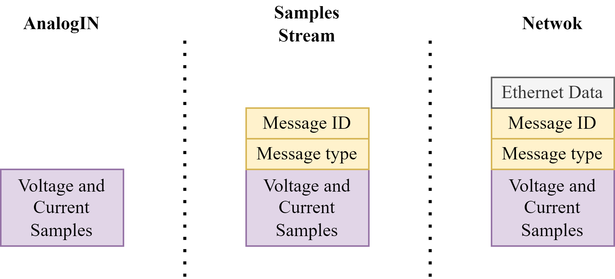
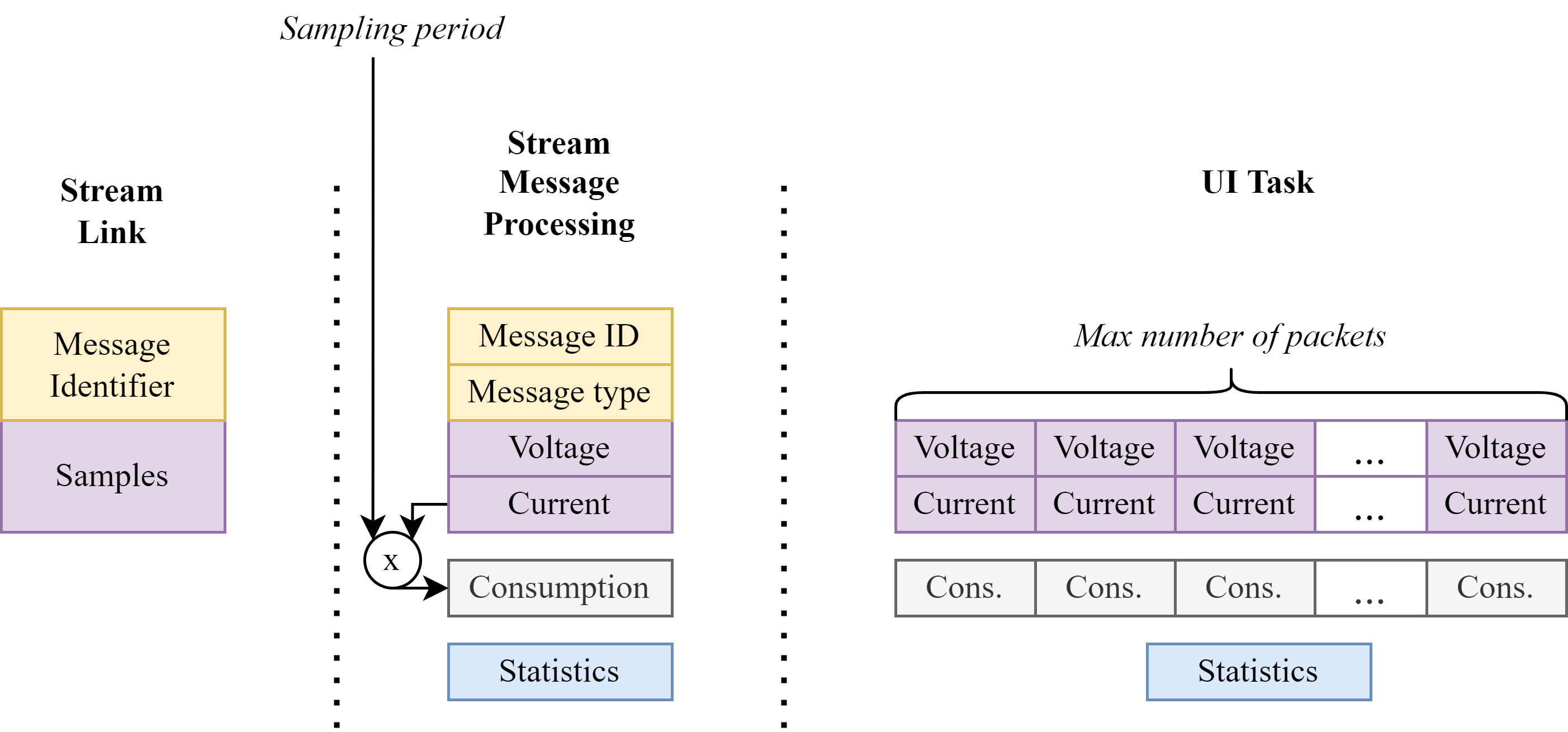
The sequential MID allows the host system to detect potential packet loss during transmission because unreliable, very fast, UDP protocol is used for packet transmission. The MTI serves to identify the specific data type contained within the packet. While the current version handles only one data type, this design offers flexibility for future implementations that may include different data streaming types. Data samples, together with MID and MTI, create a Stream message packet which is forwarded to the network service where it is encapsulated inside the corresponding ethernet packet and sent to the host side. Stream message packet creation over different software services is illustrated in Figure 3.
From Figure 2, it is obvious that two buffers, located in subsequent memory spaces, are used. This is done to achieve simultaneous data processing and transmission. In other words, while DMA fills the second buffer, the first buffer is processed and transmitted, and vice versa. To achieve this, DMA is configured in circular double buffer mode.
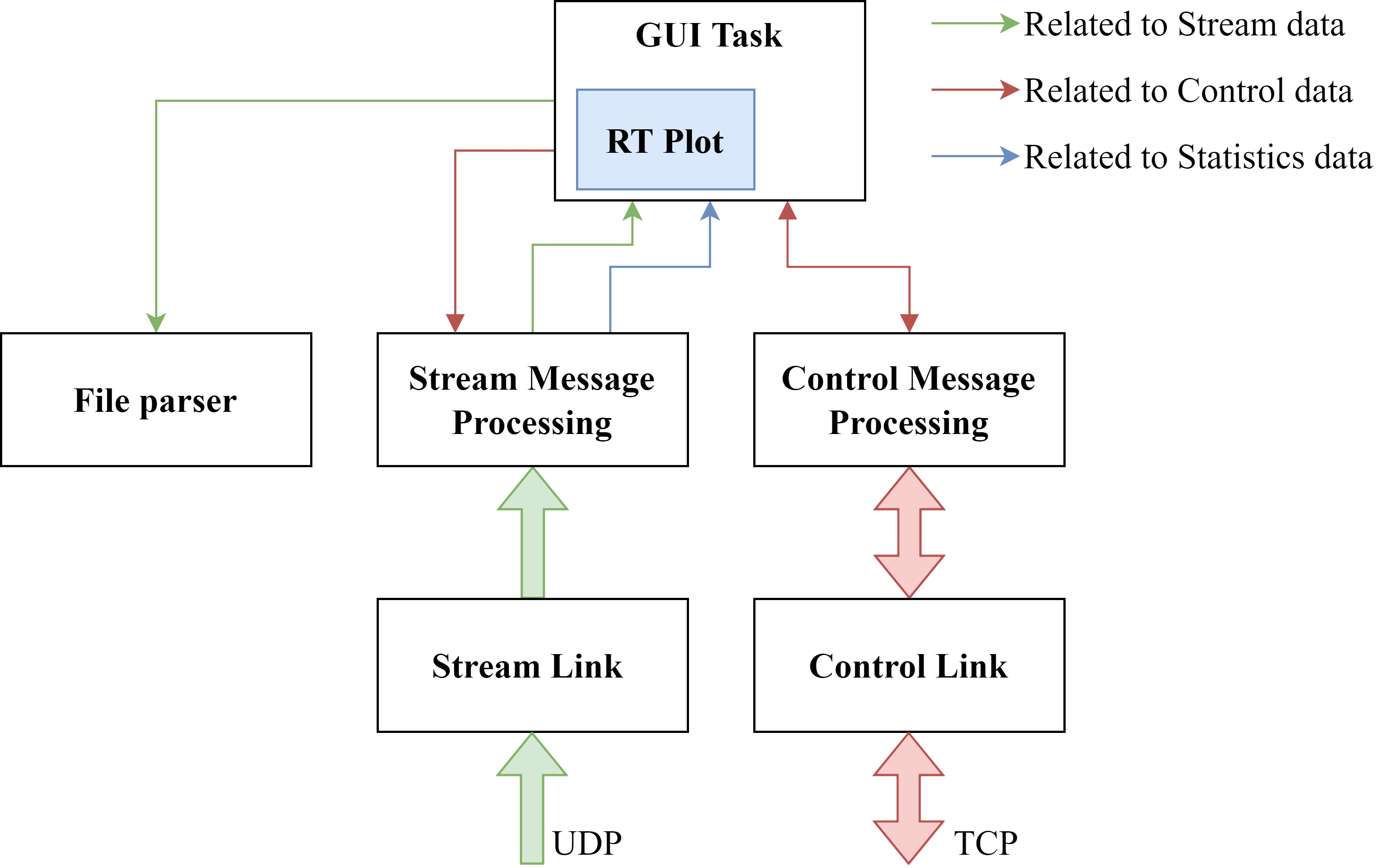
Figure 4 illustrates all GUI software blocks that are parts of streaming functionalities.
Once you launch the GUI application and successfully establish a connection with your data acquisition device, a "Device" window will appear. Here's how to configure data reception:
For optimal performance, the SMP service and SL channel operate on separate threads. They communicate with each other using a queued signal-slot connection mechanism, ensuring efficient data transfer. The device window is illustrated in Figure 5.
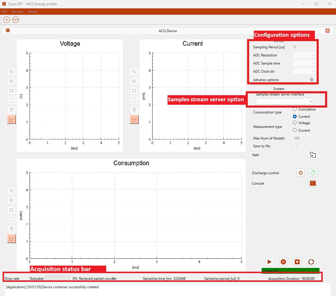
Following the selection of the network interface and the creation of the SMP service and SL channel, an initial handshake occurs between the host application and the data acquisition device. This handshake retrieves the default configuration settings from the device. Consequently, after configuration is obtained, the user can configure the following parameters:
The Device window lets you fine-tune the data acquisition process. Here's how it works:
Once the device configuration is complete, you can initiate data streaming by clicking the "Play" button within the Device window. Upon receiving this command, the acquisition device begins transmitting data samples encapsulated within Streaming Message Packets. These packets are firstly received inside the Stream Link thread where MID and MTI are extracted and together with data samples forwarded to a Stream Message Processing thread. Inside this thread are performed following actions:
Once the "Stream Message Processing" thread accumulates the maximum number of data buffers (as defined in the GUI application), it assembles everything into a single, larger data packet. This packet includes the processed data samples, along with relevant statistical information. The entire data packet is then forwarded to the main user interface (UI) task where:
Figure 7 illustrates the data flow within the GUI application
With the "Log to file" option enabled and a valid file path configured, data samples displayed in the real-time plot will be written to a corresponding log file. For each session will be created two files:
Our latest video, available on our brand-new YouTube channel, showcases the functionality of our implemented features. Since the full PCB is still under development, a signal generator was used to simulate voltage and current inputs on the STM32H755ZIQ development board. During the demonstration, the video highlights how the GUI application responds to changes in voltage and current frequency, amplitude, and offset.