Designing the OpenEPT Charger Board
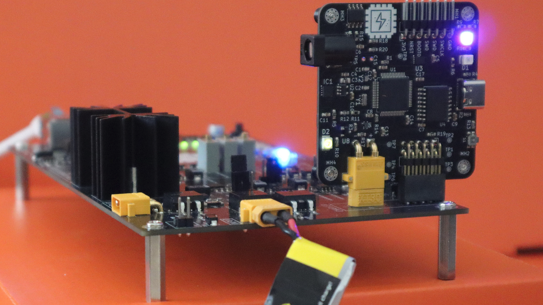
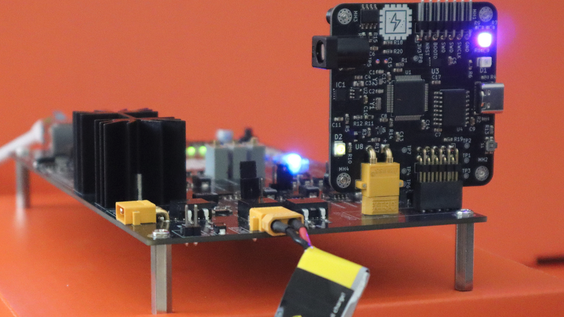
With the OpenEPT Charger Board we set out to fit power management, single-cell Li-ion charging, and an isolated USB-connected microcontroller, with 1 Kb of EEPROM on board for storing configuration. The board is a companion module for the OpenEPT evaluation platform, and from the start we designed it to be brought up, characterized, and tuned on the bench. Here's a walkthrough of the design decisions, following the design sheets.
The complete schematic for the OpenEPT Charger Board View Schematic
Sheet 1: Power, Charging, and Analog Housekeeping
Power path
For input arbitration we used a TPS2113A automatic power switch. IN1 takes 5 VDC from an external charger; IN2 takes 5V_EPP, the 5 V rail supplied by the evaluation platform. The selected source becomes the raw, unregulated +VCC rail. We set the default current limit to 1.5 A with a 330 Ω resistor, and brought the STAT pin out as STAT_POWER_SW so firmware always knows which source is feeding the board.
Downstream, +VCC gets bulk and ceramic filtering (47 µF + 100 nF) before an LP2985-33 LDO produces the regulated 3.3 V logic rail, with the usual bypass cap for low-noise operation.
The BQ25180 charger
We picked the BQ25180 as the charger because it's fully I²C-controlled: charge current, voltage, and safety limits live in firmware rather than in strapping resistors, and settings can be persisted in the on-board EEPROM. Its BAT pin routes to a standard XT30 battery connector for the Li cell, matching the EPP connector. Signal INT goes back to the MCU, and we drive the TS/MR pin through a small signal MOSFET stage (TS_MR_CHG) so the MCU can exercise temperature-sense and reset behavior.
Battery presence and voltage sensing
An LM358 covers the analog odd jobs:
- U6A works as a comparator for battery presence. One input senses the battery side through a 6.8 kΩ / 12 kΩ divider; the other sits on a 10 kΩ / 10 kΩ reference from the 3.3 V rail. We've marked the reference "to be adjusted during test" — the threshold gets dialed in on real hardware. _Note: final tested threshold values to be added after bench verification._ The output is the digital
BAT_PRESENTflag (5 V when a battery is connected), with an LED in the output path for at-a-glance indication. - U6B buffers the battery voltage. A 240 kΩ / 240 kΩ divider halves the cell voltage into the ADC range while keeping the standing drain on the battery negligible; the buffered
BAT_BUFFERoutput feeds the MCU's ADC, with a test point for probing.
Connectors, grounds, test points
The USB-C receptacle carries 5.1 kΩ pull-downs on CC1 and CC2 — standard UFP sink configuration, default USB power. VBUS and D± route off to the MCU sheet.
A 2×5 header connects to the evaluation board with I²C, UART, INT, and the 5V_EPP supply. A 5.1 kΩ pull-down on EPP_PD implements board-presence detection, so the system knows whether the platform is attached.
Grounding is where we were most deliberate: three separate domains — GNDD (digital), GNDB (battery), and GNDUSB — joined only through a net tie and the USB isolator. A bank of PWR_FLAG symbols keeps KiCad's ERC satisfied on the externally powered nets, and we exposed eight test points covering I²C, INT, all three supply rails, and the battery measurement chain:
| Test point | Net | Purpose |
|---|---|---|
| TP1 | SCL |
I²C clock |
| TP2 | SDA |
I²C data |
| TP3 | INT |
Charger interrupt line |
| TP4 | 5V_EPP |
5 V rail from the evaluation platform |
| TP5 | +VCC |
Raw rail after the TPS2113A power switch |
| TP6 | +3.3V |
Regulated logic supply |
| TP7 | BAT |
Battery rail at the charger output |
| TP8 | BAT_BUFFER |
Buffered battery voltage (LM358 output) |
Sheet 2: Microcontroller and EEPROM
STM32L476 core
An STM32L476RGTx runs the board firmware, designed to cooperate with the host EPP board. Clocking follows the classic low-power recipe: a 16 MHz ceramic resonator on the main oscillator and a 32.768 kHz crystal (7.8 pF loads) for the RTC and low-power modes. NRST and BOOT0 get 5.1 kΩ pull networks with both signals broken out, so bootloader entry is available externally.
Peripheral assignments map cleanly onto the sheet-1 signals: I²C3 shared between the charger and EEPROM, UART to the eval header, BAT_BUFFER into an ADC channel, and a fistful of digital status inputs (INT, BAT_PRESENT, EPP_PRESENT, STAT_POWER_SW, TS_MR_CHG).
MCU signal map
The full set of microcontroller signals, as wired in rev 2.3.0:
| Signal | MCU pin | Dir | Function |
|---|---|---|---|
SIGLED1 |
PA0 | Out | Signal LED D1 (via 680 Ω) |
SIGLEDR |
PA1 | Out | RGB LED, red channel (30 Ω) |
SIGLEDB |
PA2 | Out | RGB LED, blue channel (130 Ω) |
SIGLEDG |
PA3 | Out | RGB LED, green channel (56 Ω) |
INT |
PA4 | In | Interrupt from BQ25180 charger |
BAT_PRESENT |
PA6 | In | Battery presence flag from LM358 comparator |
TS_MR_CHG |
PA7 | Out | Drive for charger TS/MR pin (MOSFET stage) |
MCU_D− / MCU_D+ |
PA11 / PA12 | Bidir | USB FS data, to ADuM3160 downstream side |
SWDIO / SWCLK |
PA13 / PA14 | — | SWD debug port (J2) |
SCL / SDA |
PC0 / PC1 | Bidir | I²C3 to BQ25180 and AT24CS01 |
BAT_VOLTAGE |
PC2 | In (ADC) | Buffered, halved battery voltage (BAT_BUFFER) |
UART_TX / UART_RX |
PC10 / PC11 | Out / In | UART to evaluation-board header (named from the MCU's perspective) |
OSCL+ / OSCL− |
PC14 / PC15 | — | 32.768 kHz crystal Y2 |
OSCH+ / OSCH− |
PH0 / PH1 | — | 16 MHz ceramic resonator Y1 |
EPP_PRESENT |
PB0 | In | Evaluation-platform presence detection (EPP_PD pull-down) |
STAT_POWER_SW |
PB1 | In | Active-source status from TPS2113A |
SWO |
PB3 | Out | ITM trace to J2 |
| GP button | PB6 | In | Tactile switch S1 (5.1 kΩ pull-up) |
RST |
NRST | In | Reset, 5.1 kΩ pull-up, broken out to J2 |
BOOT0 |
BOOT0 | In | Boot mode select, 5.1 kΩ pull-down, broken out to J2 |
User I/O and debug
Status indication comes from an RGB LED with per-channel resistors of 30 Ω, 130 Ω, and 56 Ω — calculated for 10 mA per die, compensating for the different forward voltages of each color. A separate signal LED and a general-purpose tactile button round out the user interface. A 7-pin header exposes SWDIO, SWCLK, SWO, RST, and BOOT0, so we get flashing, debugging, and ITM trace from one connector.
USB isolation
Between the MCU's USB peripheral and the Type-C connector sits an ADuM3160 digital isolator. Its upstream side lives entirely in the GNDUSB domain with the connector; the downstream side sits on local 3.3 V / GNDD with the MCU's D± lines. This galvanic barrier is the whole reason for the split ground planes: faults on the battery/charger side can't reach the host PC, and ground loops between the USB host and the evaluation setup are broken by construction.
Configuration EEPROM
The 1 Kb configuration store is an AT24CS01 on the shared I²C bus, strapped to address 0b000 with write protect disabled so firmware can update configuration at runtime. As a bonus, the CS-series parts carry a factory-programmed unique serial number — each board is individually identifiable, which is handy for lab automation. _Note: the exact configuration layout (charge profiles, calibration constants, board ID) is still being defined and will be documented in a follow-up post._
Closing Thoughts
Three principles shaped this revision: software-defined charging (an I²C charger plus EEPROM turns charge profiles into data, not hardware), genuine domain separation (three grounds and a USB isolator, not just a token ferrite), and testability (eight test points, a monitored power switch, and a comparator threshold we openly expect to tune on the bench). We hope it serves as a useful reference for anyone building a battery-backed, USB-connected embedded module.
Design: Djokic D. (2026-04-09) · Check: Lakic P. (2026-04-16) · Approval: Turkmanovic H. (2026-04-25)